- 您现在的位置:买卖IC网 > Sheet目录868 > LTM4606MPV#PBF (Linear Technology)IC DC/DC UMODULE 6A 133-LGA
�� �
�
�LTM4606�
�APPLICATIONS� INFORMATION�
�Table� 3.� 1.5V� Output�
�DERATING� CURVE�
�Figures� 8,� 10�
�Figures� 8,� 10�
�Figures� 8,� 10�
�Figures� 9,� 11�
�Figures� 9,� 11�
�Figures� 9,� 11�
�V� IN� (V)�
�5,� 12�
�5,� 12�
�5,� 12�
�5,� 12�
�5,� 12�
�5,� 12�
�POWER� LOSS� CURVE�
�Figure� 6�
�Figure� 6�
�Figure� 6�
�Figure� 6�
�Figure� 6�
�Figure� 6�
�AIR� FLOW� (LFM)�
�0�
�200�
�400�
�0�
�200�
�400�
�HEAT� SINK�
�None�
�None�
�None�
�BGA� Heat� Sink�
�BGA� Heat� Sink�
�BGA� Heat� Sink�
�θ� JA� (°C/W)�
�13.5�
�10�
�9�
�9.5�
�7�
�5�
�Table� 4.� 3.3V� Output�
�DERATING� CURVE�
�Figures� 12,� 14�
�Figures� 12,� 14�
�Figures� 12,� 14�
�Figures� 13,� 15�
�Figures� 13,� 15�
�Figures� 13,� 15�
�V� IN� (V)�
�12,� 24�
�12,� 24�
�12,� 24�
�12,� 24�
�12,� 24�
�12,� 24�
�POWER� LOSS� CURVE�
�Figure� 7�
�Figure� 7�
�Figure� 7�
�Figure� 7�
�Figure� 7�
�Figure� 7�
�AIR� FLOW� (LFM)�
�0�
�200�
�400�
�0�
�200�
�400�
�HEAT� SINK�
�None�
�None�
�None�
�BGA� Heat� Sink�
�BGA� Heat� Sink�
�BGA� Heat� Sink�
�θ� JA� (°C/W)�
�13.5�
�11�
�10�
�10�
�7�
�5�
�Heat� Sink� Manufacturer�
�AAVID� Thermalloy�
�Cool� Innovations�
�PART� NUMBER�
�375424B00034G�
�4-050503P� to� 4-050508P�
�WEBSITE�
�www.aavidthermalloy.com�
�www.cooinnovations.com�
�C� IN�
�C� IN�
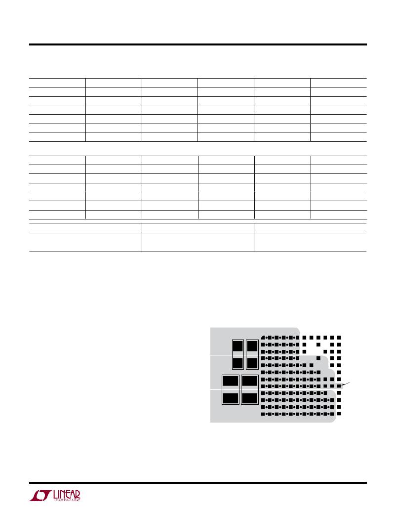
�Layout� Checklist/Example�
�The� high� integration� of� LTM4606� makes� the� PCB� board�
�layout� very� simple� and� easy.� However,� to� optimize� its�
�electrical� and� thermal� performance,� some� layout� con-�
�siderations� are� still� necessary.�
�?� Use� large� PCB� copper� areas� for� high� current� path,� in� -�
�cluding� V� IN� ,� PGND� and� V� OUT� .� It� helps� to� minimize� the�
�PCB� conduction� loss� and� thermal� stress.�
�?� Place� high� frequency� ceramic� input� and� output� capaci� -�
�tors� next� to� the� V� D� ,� PGND� and� V� OUT� pins� to� minimize�
�high� frequency� noise.�
�?� Place� a� dedicated� power� ground� layer� underneath� the�
�unit.�
�?� Use� a� separated� SGND� ground� copper� area� for� com� -�
�ponents� connected� to� signal� pins.� Connect� the� SGND�
�to� PGND� underneath� the� unit.�
�?� Place� one� or� more� high� frequency� ceramic� capacitors�
�close� to� the� connection� into� the� system� board.�
�Figure� 17� gives� a� good� example� of� the� recommended� layout.�
�V� IN�
�PGND�
�SIGNAL�
�GND�
�?� Use� round� corners� for� the� PCB� copper� layer� to� minimize�
�the� radiated� noise.�
�C� OUT�
�C� OUT�
�?� To� minimize� the� EMI� noise� and� reduce� module� thermal�
�stress,� use� multiple� vias� for� interconnection� between�
�top� layer� and� other� power� layers� on� different� locations.�
�?� Do� not� put� vias� directly� on� pads,� unless� they� are� capped.�
�V� OUT�
�(LGA� Shown,� for� BGA� Use� Circle� Pads)�
�Figure� 17.� Recommended� PCB� Layout�
�4606� F17�
�4606fd�
�For� more� information� www.linear.com/LTM4606�
�19�
�发布紧急采购,3分钟左右您将得到回复。
相关PDF资料
LTM4607IV#PBF
IC BUCK/BOOST SYNC ADJ 5A 141LGA
LTM4608AEV#PBF
IC BUCK SYNC ADJ 8A 68LGA
LTM4608IV#PBF
IC DC/DC UMODULE 8A 68-LGA
LTM4609IV#PBF
IC BUCK/BOOST SYNC ADJ 4A 141LGA
LTM4612IV#PBF
IC BUCK SYNC ADJ 5A 133LGA
LTM4613MPV#PBF
IC UMODULE DC/DC 8A 133-LGA
LTM4614IV#PBF
IC UMODULE DC/DC DUAL 4A 144LGA
LTM4615IV#PBF
IC SWIT REG BUCK 4A ADJ 144LGA
相关代理商/技术参数
LTM4606MPV-PBF
制造商:LINER 制造商全称:Linear Technology 功能描述:Ultralow EMI 28VIN, 6A DC/DC μModule
LTM4606V
制造商:LIN 功能描述:MODULE 133-LGA LINEAR, 0843
LTM4607
制造商:LINER 制造商全称:Linear Technology 功能描述:High Effi ciency, Synchronous, 4-Switch Buck-Boost Controller
LTM4607EV#PBF
功能描述:IC BUCK/BOOST SYNC ADJ 5A 141LGA RoHS:是 类别:电源 - 板载 >> DC DC Converters 系列:µModule® 设计资源:VI-200, VI-J00 Design Guide, Appl Manual 标准包装:1 系列:* 类型:隔离 输出数:1 电压 - 输入(最小):66V 电压 - 输入(最大):160V Voltage - Output 1:12V Voltage - Output 2:- Voltage - Output 3:- 电流 - 输出(最大):* 电源(瓦) - 制造商系列:50W 电压 - 隔离:* 特点:* 安装类型:通孔 封装/外壳:9-FinMod 尺寸/尺寸:4.60" L x 1.86" W x 0.79" H(116.8mm x 47.2mm x 20.1mm) 包装:散装 工作温度:-25°C ~ 85°C 效率:* 电源(瓦特)- 最大:*
LTM4607EV#PBF
制造商:Linear Technology 功能描述:DC/DC Converter IC
LTM4607EVPBF
制造商:Linear Technology 功能描述:Conv DC-DC Step Up Step Down
LTM4607EV-PBF
制造商:LINER 制造商全称:Linear Technology 功能描述:36VIN, 24VOUT High Effi ciency Buck-Boost DC/DC μModule
LTM4607IV#PBF
功能描述:IC BUCK/BOOST SYNC ADJ 5A 141LGA RoHS:是 类别:电源 - 板载 >> DC DC Converters 系列:µModule® 设计资源:VI-200, VI-J00 Design Guide, Appl Manual 标准包装:1 系列:* 类型:隔离 输出数:1 电压 - 输入(最小):66V 电压 - 输入(最大):160V Voltage - Output 1:12V Voltage - Output 2:- Voltage - Output 3:- 电流 - 输出(最大):* 电源(瓦) - 制造商系列:50W 电压 - 隔离:* 特点:* 安装类型:通孔 封装/外壳:9-FinMod 尺寸/尺寸:4.60" L x 1.86" W x 0.79" H(116.8mm x 47.2mm x 20.1mm) 包装:散装 工作温度:-25°C ~ 85°C 效率:* 电源(瓦特)- 最大:*